
Infineon Expands CoolMOS CFD7A Line with QDPAK Package for Enhanced EV Charging Efficiency
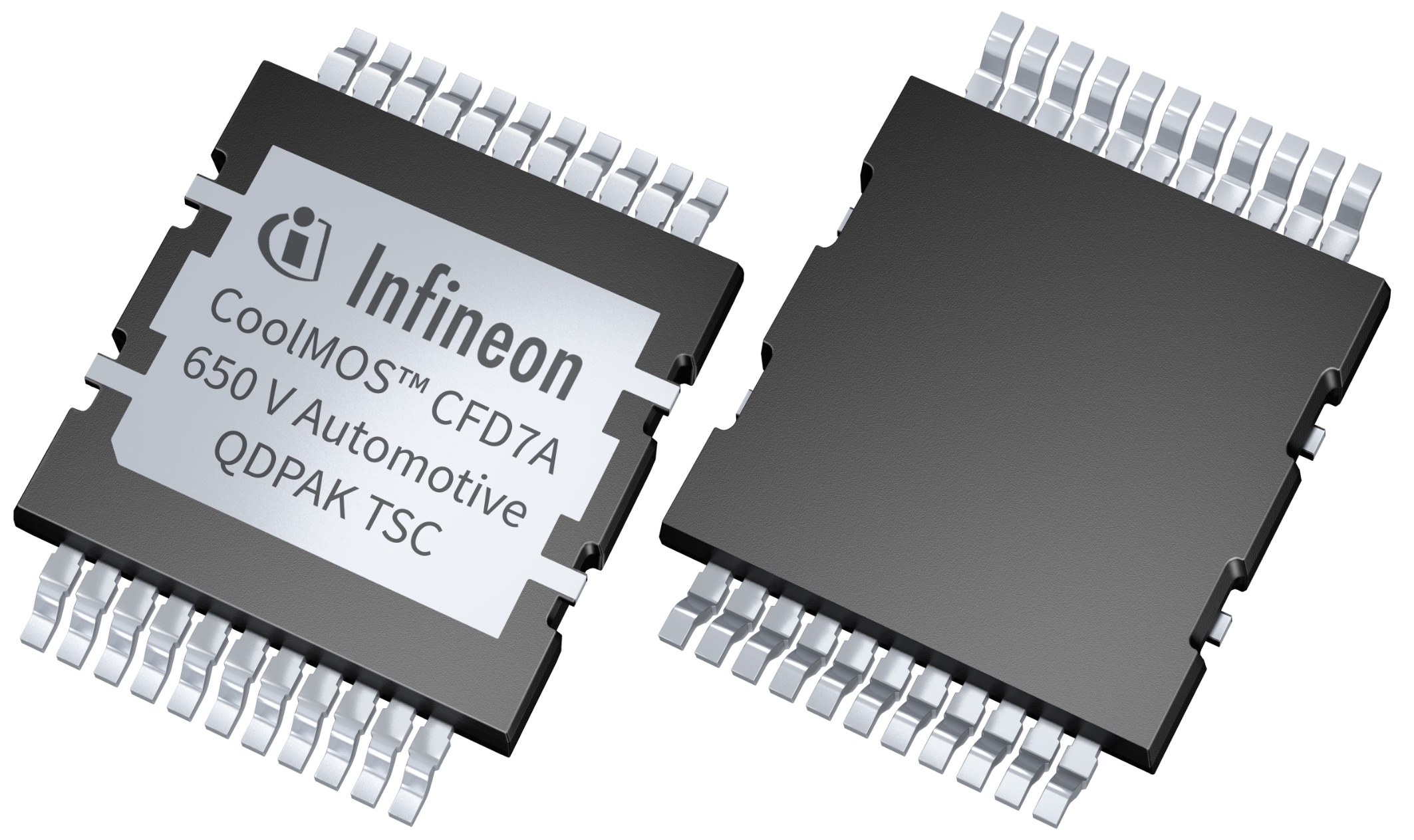
(IN BRIEF) Infineon Technologies AG is extending its 650 V CoolMOS™ CFD7A series by introducing the QDPAK package to meet the growing demand for efficient and high-performance power electronics in electric vehicle (EV) charging systems. The QDPAK package offers equivalent thermal capabilities while improving electrical performance over existing TO247 THD devices. This advancement supports energy-efficient onboard chargers and DC-DC converters, ultimately reducing charging times, vehicle weight, and total ownership costs for EVs. The CoolMOS CFD7A series enhances high-voltage applications with features such as reduced parasitic source inductance, minimized electromagnetic interference (EMI), precise current sensing with a Kelvin source pin, high current capability, and high power dissipation (P tot) of up to 694 W at 25°C. The QDPAK TSC (top side cooled) variant facilitates higher power densities and efficient PCB space utilization, simplifying assembly and reducing system costs. The package also addresses thermal limitations, contributing to a cost-effective and robust solution suitable for modern power requirements. Furthermore, the QDPAK TSC package has become a JEDEC standard for high-power applications, promoting widespread adoption, and additional Automotive Qualified devices are planned for release in 2024, including 750 V and 1200 V CoolSiC™ devices. Both top-side cooled (TSC) and bottom-side cooled (BSC) variants of the 650 V CoolMOS CFD7A in the QDPAK package are currently available for order. More details can be found on Infineon’s website.
(PRESS RELEASE) MUNICH, 23-Nov-2023 — /EuropaWire/ — The accelerated transition to electric vehicles has led to significant innovations in charging systems that demand more cost-efficient and high performing power electronics. Addressing this, Infineon Technologies AG (FSE: IFX / OTCQX: IFNNY) expands its 650 V CoolMOS™ CFD7A portfolio by introducing the QDPAK package. This package family is designed to provide equivalent thermal capabilities with improved electrical performance over the well-known TO247 THD devices, thus enabling efficient energy utilization in onboard chargers and DC-DC converters.
Efficient and powerful electric vehicle charging systems help reduce charging times and vehicle weight, increasing design flexibility and reduce the total cost of ownership of the vehicle. This new addition complements the existing CoolMOS CFD7A series, offering versatility with top-side and bottom-side cooled packages. The QDPAK TSC (top side cooled), enables designers to achieve higher power densities and optimal PCB space utilization.
The 650 V CoolMOS CFD7A offers several important features for reliable operation in high-voltage applications. Thanks to its reduced parasitic source inductance, the device can minimize electromagnetic interference (EMI), ensuring clear signals and consistent performance. The Kelvin source pin also provides improved precision for current sensing, ensuring accurate measurements even in challenging conditions. With a creepage distance suitable for high voltage applications, as well as high current capability and high power dissipation (P tot) of up to 694 W at 25°C, it is a versatile and powerful device for a wide range of high-voltage applications.
New system designs using 650 V CoolMOS CFD7A in QDPAK TSC will maximize PCB space use, doubling power density and enhancing thermal management via substrate thermal decoupling. This approach simplifies assembly, eliminates board stacking and reduces the need for connectors, thereby lowering system costs. The power switch reduces thermal resistance by up to 35 percent, providing high power dissipation that outperforms standard cooling solutions.
This feature overcomes the thermal limitations of bottom side cooled SMD designs using FR4 PCBs, resulting in a significant boost in system performance. The optimized power loop design locates drivers near the power switch, improving reliability by reducing stray inductance and chip temperatures. Overall, these features contribute to a cost-effective, robust, and efficient system ideal for modern power needs.
As announced in February 2023, the QDPAK TSC package has been registered as a JEDEC standard for high-power applications, helping to establish a broad adoption of TSC in new designs with one standard package design and footprint. To further to accelerate this transition, Infineon will also release additional Automotive Qualified devices in QDPAK TSC for onboard chargers and DC-DC converters in 2024, such as 750 V and 1200 V CoolSiC™ devices.
Availability
The 650 V CoolMOS CFD7A is available in QDPAK package with two versions, top-side cooled (TSC) and bottom-side cooled (BSC). Both variants can be ordered now. More information is available at www.infineon.com/cfd7a.
Media Contact:
Reinhard von Faltin
Tel: +49 89 234 39694
mailto: Reinhard.vonFaltin@infineon.com
SOURCE: Infineon
MORE ON INFINEON, ETC.:
- Aortic Aneurysms: EU-funded Pandora Project Brings In-Silico Modelling to Aid Surgeons
- BREAKING NEWS: New Podcast “Spreading the Good BUZZ” Hosted by Josh and Heidi Case Launches July 7th with Explosive Global Reach and a Mission to Transform Lives Through Hope and Community in Recovery
- Cha Cha Cha kohtub krüptomaailmaga: Winz.io teeb koostööd Euroopa visionääri ja staari Käärijäga
- Digi Communications N.V. announces Conditional stock options granted to Executive Directors of the Company, for the year 2025, based on the general shareholders’ meeting approval from 25 June 20244
- Cha Cha Cha meets crypto: Winz.io partners with European visionary star Käärijä
- Digi Communications N.V. announces the exercise of conditional share options by the executive directors of the Company, for the year 2024, as approved by the Company’s OGSM from 25 June 2024
- “Su Fortuna Se Ha Construido A Base de La Defraudación Fiscal”: Críticas Resurgen Contra Ricardo Salinas en Medio de Nuevas Revelaciones Judiciales y Fiscaleso
- Digi Communications N.V. announces the availability of the instruction regarding the payment of share dividend for the 2024 financial year
- SOILRES project launches to revive Europe’s soils and future-proof farming
- Josh Case, ancien cadre d’ENGIE Amérique du Nord, PDG de Photosol US Renewable Energy et consultant d’EDF Amérique du Nord, engage aujourd’hui toute son énergie dans la lutte contre la dépendance
- Bizzy startet den AI Sales Agent in Deutschland: ein intelligenter Agent zur Automatisierung der Vertriebspipeline
- Bizzy lance son agent commercial en France : un assistant intelligent qui automatise la prospection
- Bizzy lancia l’AI Sales Agent in Italia: un agente intelligente che automatizza la pipeline di vendita
- Bizzy lanceert AI Sales Agent in Nederland: slimme assistent automatiseert de sales pipeline
- Bizzy startet AI Sales Agent in Österreich: ein smarter Agent, der die Sales-Pipeline automatisiert
- Bizzy wprowadza AI Sales Agent w Polsce: inteligentny agent, który automatyzuje budowę lejka sprzedaży
- Bizzy lanza su AI Sales Agent en España: un agente inteligente que automatiza la generación del pipeline de ventas
- Bizzy launches AI Sales Agent in the UK: a smart assistant that automates sales pipeline generation
- As Sober.Buzz Community Explodes Its Growth Globally it is Announcing “Spreading the Good BUZZ” Podcast Hosted by Josh Case Debuting July 7th
- Digi Communications N.V. announces the OGMS resolutions and the availability of the approved 2024 Annual Report
- Escándalo Judicial en Aumento Alarma a la Opinión Pública: Suprema Corte de México Enfrenta Acusaciones de Favoritismo hacia el Aspirante a Magnate Ricardo Salinas Pliego
- Winz.io Named AskGamblers’ Best Casino 2025
- Kissflow Doubles Down on Germany as a Strategic Growth Market with New AI Features and Enterprise Focus
- Digi Communications N.V. announces Share transaction made by a Non-Executive Director of the Company with class B shares
- Salinas Pliego Intenta Frenar Investigaciones Financieras: UIF y Expertos en Corrupción Prenden Alarmas
- Digital integrity at risk: EU Initiative to strengthen the Right to be forgotten gains momentum
- Orden Propuesta De Arresto E Incautación Contra Ricardo Salinas En Corte De EE.UU
- Digi Communications N.V. announced that Serghei Bulgac, CEO and Executive Director, sold 15,000 class B shares of the company’s stock
- PFMcrypto lancia un sistema di ottimizzazione del reddito basato sull’intelligenza artificiale: il mining di Bitcoin non è mai stato così facile
- Azteca Comunicaciones en Quiebra en Colombia: ¿Un Presagio para Banco Azteca?
- OptiSigns anuncia su expansión Europea
- OptiSigns annonce son expansion européenne
- OptiSigns kündigt europäische Expansion an
- OptiSigns Announces European Expansion
- Digi Communications NV announces release of Q1 2025 financial report
- Banco Azteca y Ricardo Salinas Pliego: Nuevas Revelaciones Aumentan la Preocupación por Riesgos Legales y Financieros
- Digi Communications NV announces Investors Call for the presentation of the Q1 2025 Financial Results
- Digi Communications N.V. announces the publication of the 2024 Annual Financial Report and convocation of the Company’s general shareholders meeting for June 18, 2025, for the approval of, among others, the 2024 Annual Financial Report, available on the Company’s website
- La Suprema Corte Sanciona a Ricardo Salinas de Grupo Elektra por Obstrucción Legal
- Digi Communications N.V. announces the conclusion of an Incremental to the Senior Facilities Agreement dated 21 April 2023
- 5P Europe Foundation: New Initiative for African Children
- 28-Mar-2025: Digi Communications N.V. announces the conclusion of Facilities Agreements by companies within Digi Group
- Aeroluxe Expeditions Enters U.S. Market with High-Touch Private Jet Journeys—At a More Accessible Price ↗️
- SABIO GROUP TAKES IT’S ‘DISRUPT’ CX PROGRAMME ACROSS EUROPE
- EU must invest in high-quality journalism and fact-checking tools to stop disinformation
- ¿Está Banco Azteca al borde de la quiebra o de una intervención gubernamental? Preocupaciones crecientes sobre la inestabilidad financiera
- Netmore and Zenze Partner to Deploy LoRaWAN® Networks for Cargo and Asset Monitoring at Ports and Terminals Worldwide
- Rise Point Capital: Co-investing with Independent Sponsors to Unlock International Investment Opportunities
- Netmore Launches Metering-as-a-Service to Accelerate Smart Metering for Water and Gas Utilities
- Digi Communications N.V. announces that a share transaction was made by a Non-Executive Director of the Company with class B shares
- La Ballata del Trasimeno: Il Mediometraggio si Trasforma in Mini Serie
- Digi Communications NV Announces Availability of 2024 Preliminary Financial Report
- Digi Communications N.V. announces the recent evolution and performance of the Company’s subsidiary in Spain
- BevZero Equipment Sales and Distribution Enhances Dealcoholization Capabilities with New ClearAlc 300 l/h Demonstration Unit in Spain Facility
- Digi Communications NV announces Investors Call for the presentation of the 2024 Preliminary Financial Results
- Reuters webinar: Omnibus regulation Reuters post-analysis
- Patients as Partners® Europe Launches the 9th Annual Event with 2025 Keynotes, Featured Speakers and Topics
- eVTOLUTION: Pioneering the Future of Urban Air Mobility
- Reuters webinar: Effective Sustainability Data Governance
- Las acusaciones de fraude contra Ricardo Salinas no son nuevas: una perspectiva histórica sobre los problemas legales del multimillonario
- Digi Communications N.V. Announces the release of the Financial Calendar for 2025
- USA Court Lambasts Ricardo Salinas Pliego For Contempt Of Court Order
- 3D Electronics: A New Frontier of Product Differentiation, Thinks IDTechEx
- Ringier Axel Springer Polska Faces Lawsuit for Over PLN 54 million
- Digi Communications N.V. announces the availability of the report on corporate income tax information for the financial year ending December 31, 2023
- Unlocking the Multi-Million-Dollar Opportunities in Quantum Computing
- Digi Communications N.V. Announces the Conclusion of Facilities Agreements by Companies within Digi Group
- The Hidden Gem of Deep Plane Facelifts
- KAZANU: Redefining Naturist Hospitality in Saint Martin ↗️
- New IDTechEx Report Predicts Regulatory Shifts Will Transform the Electric Light Commercial Vehicle Market
- Almost 1 in 4 Planes Sold in 2045 to be Battery Electric, Finds IDTechEx Sustainable Aviation Market Report
- Digi Communications N.V. announces the release of Q3 2024 financial results
- Digi Communications NV announces Investors Call for the presentation of the Q3 2024 Financial Results
- Pilot and Electriq Global announce collaboration to explore deployment of proprietary hydrogen transport, storage and power generation technology
- Digi Communications N.V. announces the conclusion of a Memorandum of Understanding by its subsidiary in Romania
- Digi Communications N.V. announces that the Company’s Portuguese subsidiary finalised the transaction with LORCA JVCO Limited
- Digi Communications N.V. announces that the Portuguese Competition Authority has granted clearance for the share purchase agreement concluded by the Company’s subsidiary in Portugal
- OMRON Healthcare introduceert nieuwe bloeddrukmeters met AI-aangedreven AFib-detectietechnologie; lancering in Europa september 2024
- OMRON Healthcare dévoile de nouveaux tensiomètres dotés d’une technologie de détection de la fibrillation auriculaire alimentée par l’IA, lancés en Europe en septembre 2024
- OMRON Healthcare presenta i nuovi misuratori della pressione sanguigna con tecnologia di rilevamento della fibrillazione atriale (AFib) basata sull’IA, in arrivo in Europa a settembre 2024
- OMRON Healthcare presenta los nuevos tensiómetros con tecnología de detección de fibrilación auricular (FA) e inteligencia artificial (IA), que se lanzarán en Europa en septiembre de 2024
- Alegerile din Moldova din 2024: O Bătălie pentru Democrație Împotriva Dezinformării
- Northcrest Developments launches design competition to reimagine 2-km former airport Runway into a vibrant pedestrianized corridor, shaping a new era of placemaking on an international scale
- The Road to Sustainable Electric Motors for EVs: IDTechEx Analyzes Key Factors
- Infrared Technology Breakthroughs Paving the Way for a US$500 Million Market, Says IDTechEx Report
- MegaFair Revolutionizes the iGaming Industry with Skill-Based Games
- European Commission Evaluates Poland’s Media Adherence to the Right to be Forgotten
- Global Race for Autonomous Trucks: Europe a Critical Region Transport Transformation
- Digi Communications N.V. confirms the full redemption of €450,000,000 Senior Secured Notes
- AT&T Obtiene Sentencia Contra Grupo Salinas Telecom, Propiedad de Ricardo Salinas, Sus Abogados se Retiran Mientras Él Mueve Activos Fuera de EE.UU. para Evitar Pagar la Sentencia
- Global Outlook for the Challenging Autonomous Bus and Roboshuttle Markets
- Evolving Brain-Computer Interface Market More Than Just Elon Musk’s Neuralink, Reports IDTechEx
- Latin Trails Wraps Up a Successful 3rd Quarter with Prestigious LATA Sustainability Award and Expands Conservation Initiatives ↗️
- Astor Asset Management 3 Ltd leitet Untersuchung für potenzielle Sammelklage gegen Ricardo Benjamín Salinas Pliego von Grupo ELEKTRA wegen Marktmanipulation und Wertpapierbetrug ein
- Digi Communications N.V. announces that the Company’s Romanian subsidiary exercised its right to redeem the Senior Secured Notes due in 2025 in principal amount of €450,000,000
- Astor Asset Management 3 Ltd Inicia Investigación de Demanda Colectiva Contra Ricardo Benjamín Salinas Pliego de Grupo ELEKTRA por Manipulación de Acciones y Fraude en Valores
- Astor Asset Management 3 Ltd Initiating Class Action Lawsuit Inquiry Against Ricardo Benjamín Salinas Pliego of Grupo ELEKTRA for Stock Manipulation & Securities Fraud
- Digi Communications N.V. announced that its Spanish subsidiary, Digi Spain Telecom S.L.U., has completed the first stage of selling a Fibre-to-the-Home (FTTH) network in 12 Spanish provinces
- Natural Cotton Color lancia la collezione "Calunga" a Milano
- Astor Asset Management 3 Ltd: Salinas Pliego Incumple Préstamo de $110 Millones USD y Viola Regulaciones Mexicanas
- Astor Asset Management 3 Ltd: Salinas Pliego Verstößt gegen Darlehensvertrag über 110 Mio. USD und Mexikanische Wertpapiergesetze
- ChargeEuropa zamyka rundę finansowania, której przewodził fundusz Shift4Good tym samym dokonując historycznej francuskiej inwestycji w polski sektor elektromobilności
- Strengthening EU Protections: Robert Szustkowski calls for safeguarding EU citizens’ rights to dignity
- Digi Communications NV announces the release of H1 2024 Financial Results
- Digi Communications N.V. announces that conditional stock options were granted to a director of the Company’s Romanian Subsidiary
- Digi Communications N.V. announces Investors Call for the presentation of the H1 2024 Financial Results
- Digi Communications N.V. announces the conclusion of a share purchase agreement by its subsidiary in Portugal
- Digi Communications N.V. Announces Rating Assigned by Fitch Ratings to Digi Communications N.V.
- Digi Communications N.V. announces significant agreements concluded by the Company’s subsidiaries in Spain
- SGW Global Appoints Telcomdis as the Official European Distributor for Motorola Nursery and Motorola Sound Products
- Digi Communications N.V. announces the availability of the instruction regarding the payment of share dividend for the 2023 financial year
- Digi Communications N.V. announces the exercise of conditional share options by the executive directors of the Company, for the year 2023, as approved by the Company’s Ordinary General Shareholders’ Meetings from 18th May 2021 and 28th December 2022
- Digi Communications N.V. announces the granting of conditional stock options to Executive Directors of the Company based on the general shareholders’ meeting approval from 25 June 2024
- Digi Communications N.V. announces the OGMS resolutions and the availability of the approved 2023 Annual Report
- Czech Composer Tatiana Mikova Presents Her String Quartet ‘In Modo Lidico’ at Carnegie Hall
- SWIFTT: A Copernicus-based forest management tool to map, mitigate, and prevent the main threats to EU forests
- WickedBet Unveils Exciting Euro 2024 Promotion with Boosted Odds
- Museum of Unrest: a new space for activism, art and design
- Digi Communications N.V. announces the conclusion of a Senior Facility Agreement by companies within Digi Group
- Digi Communications N.V. announces the agreements concluded by Digi Romania (formerly named RCS & RDS S.A.), the Romanian subsidiary of the Company
- Green Light for Henri Hotel, Restaurants and Shops in the “Alter Fischereihafen” (Old Fishing Port) in Cuxhaven, opening Summer 2026
- Digi Communications N.V. reports consolidated revenues and other income of EUR 447 million, adjusted EBITDA (excluding IFRS 16) of EUR 140 million for Q1 2024
- Digi Communications announces the conclusion of Facilities Agreements by companies from Digi Group
- Digi Communications N.V. Announces the convocation of the Company’s general shareholders meeting for 25 June 2024 for the approval of, among others, the 2023 Annual Report
- Digi Communications NV announces Investors Call for the presentation of the Q1 2024 Financial Results
- Digi Communications intends to propose to shareholders the distribution of dividends for the fiscal year 2023 at the upcoming General Meeting of Shareholders, which shall take place in June 2024
- Digi Communications N.V. announces the availability of the Romanian version of the 2023 Annual Report
- Digi Communications N.V. announces the availability of the 2023 Annual Report
- International Airlines Group adopts Airline Economics by Skailark ↗️
- BevZero Spain Enhances Sustainability Efforts with Installation of Solar Panels at Production Facility
- Digi Communications N.V. announces share transaction made by an Executive Director of the Company with class B shares
- BevZero South Africa Achieves FSSC 22000 Food Safety Certification
- Digi Communications N.V.: Digi Spain Enters Agreement to Sell FTTH Network to International Investors for Up to EUR 750 Million
- Patients as Partners® Europe Announces the Launch of 8th Annual Meeting with 2024 Keynotes and Topics
- driveMybox continues its international expansion: Hungary as a new strategic location
- Monesave introduces Socialised budgeting: Meet the app quietly revolutionising how users budget
- Digi Communications NV announces the release of the 2023 Preliminary Financial Results
- Digi Communications NV announces Investors Call for the presentation of the 2023 Preliminary Financial Results
- Lensa, един от най-ценените търговци на оптика в Румъния, пристига в България. Първият шоурум е открит в София
- Criando o futuro: desenvolvimento da AENO no mercado de consumo em Portugal
- Digi Communications N.V. Announces the release of the Financial Calendar for 2024
- Customer Data Platform Industry Attracts New Participants: CDP Institute Report
- eCarsTrade annonce Dirk Van Roost au poste de Directeur Administratif et Financier: une décision stratégique pour la croissance à venir
- BevZero Announces Strategic Partnership with TOMSA Desil to Distribute equipment for sustainability in the wine industry, as well as the development of Next-Gen Dealcoholization technology
- Editor's pick archive....